The next time you place your coffee order, imagine slapping onto your to-go cup a sticker that acts as an electronic decal, letting you know the precise temperature of your triple-venti no-foam latte. Someday, the high-tech stamping that produces such a sticker might also bring us food packaging that displays a digital countdown to warn of spoiling produce, or even a window pane that shows the day’s forecast, based on measurements of the weather conditions outside.
Engineers at MIT have invented a fast, precise printing process that may make such electronic surfaces an inexpensive reality. In a paper published in Science Advances, the researchers report that they have fabricated a stamp made from forests of carbon nanotubes that is able to print electronic inks onto rigid and flexible surfaces.
A. John Hart, the Mitsui Career Development Associate Professor in Contemporary Technology and Mechanical Engineering at MIT, says the team’s stamping process should be able to print transistors small enough to control individual pixels in high-resolution displays and touchscreens. The new printing technique may also offer a relatively cheap, fast way to manufacture electronic surfaces for as-yet-unknown applications.
“There is a huge need for printing of electronic devices that are extremely inexpensive but provide simple computations and interactive functions,” Hart says. “Our new printing process is an enabling technology for high-performance, fully printed electronics, including transistors, optically functional surfaces, and ubiquitous sensors.”
It’s not the first time something like this was attempted. Other teams have tried to print electronics using inkjet printing and rubber stamping techniques but results have generally been fuzzy – literally. Because the printing is very hard to control at small scales, the technique tends to produce “coffee-ring” botches, with the ink spilling outside the borders leading to incomplete or aberrant circuits.
“There are critical limitations to existing printing processes in the control they have over the feature size and thickness of the layer that’s printed,” Hart says. “For something like a transistor or thin film with particular electrical or optical properties, those characteristics are very important.”
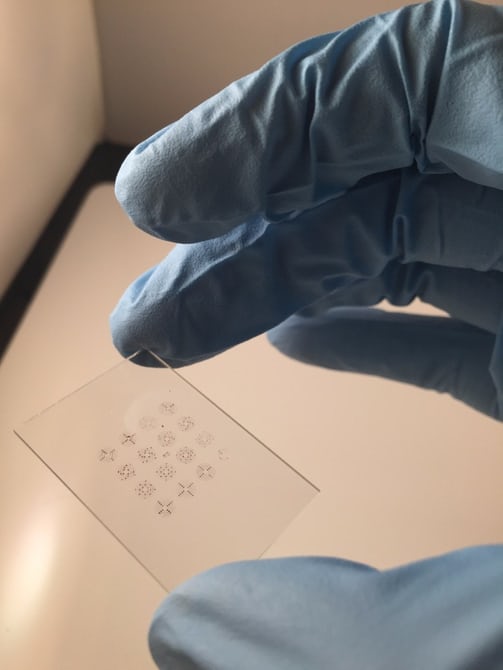
This new technology uses “nanoporous” stamps to remedy that issue. Imagine a small, spongy stamp half the size of a normal fingernail, with pores thinner than the width of a human hair. These pores allow the “ink” to flow uniformly and ensure the printing precision and achieving very high resolution. The stamp itself is fabricated from carbon nanotubes – strong, microscopic sheets of carbon atoms, arranged in cylinders – arranged in forest-like patterns.
Source: news.mit.edu