Electronics is based on measuring the tiny electrical charge of electrons passing through electronic circuits. Conventional electronic devices rely on the transport of electrical charge carriers - electrons - in a semiconductor such as silicon. Now, however, physicists are trying to exploit the 'spin' of the electron rather than its charge to create a remarkable new generation of 'spintronic' devices which will be smaller, more versatile and more robust than those currently making up silicon chips and circuit elements.
As electronics approaches the limits of silicon, spintronic components will play an important role in ensuring we enjoy steady performance gains, and faster, higher-capacity storage at lower power and cost. Magnetoelectronics, Spin Electronics, and Spintronics are different names for the same thing: the use of electrons' spins in information circuits. Spintronics offers opportunities for a new generation of devices combining standard microelectronics with spin-dependent effects that arise from the interaction between spin of the carrier and the magnetic properties of the material. This article presents a new paradigm of electronics based on the spin degree of freedom of the electron.
Working of spintronics
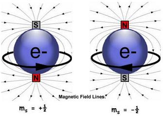
We know that an electron spins on its own axis while rotating around an atom’s nucleus. Spin can be measured because it generates tiny magnetic fields. Spin is either “up” or “down”. In the same way traditional electronics uses charge to represent information as zeros and ones, the two spin states can be used to represent the same binary data in spintronics. Traditional approaches to using spin are based on the alignment of a spin (either “up” or “down”) relative to a reference (an applied magnetic field or magnetization orientation of the ferromagnetic film). All spintronic devices act according to the simple scheme: information is stored (written) into spins as a particular spin orientation (up or down), the spins, being attached to mobile electrons, carry the information along a wire, and the information is read at a terminal.
Advantages
Spintronics is the new science of computers and memory chips that are based on electron spin rather than the charge (used in electronics). Spintronics is an exciting field that holds promise to build faster and more efficient computers and other devices. Spin orientation of conduction electrons survives for a relatively long time (nanoseconds, compared to tens of femtoseconds during which electron momentum decays), which makes spintronic devices particularly attractive for memory storage and magnetic sensors applications, and, potentially for quantum computing where electron spin would represent a bit (called qubit) of information. Spintronics has several advantages over conventional electronics. Electronics require specialized semiconductor materials in order to control the flow of charge through the transistors. But spin can be measured very simply in common metals such as copper or aluminium. Less energy is needed to change spin than to generate a current to maintain electron charges in a device, so spintronics devices use less power. Spin states can be set quickly, which makes transferring data quicker. And because electron spin is not energy-dependent, spin is non-volatile – information sent using spin remains fixed even after loss of power. Device operations proceed with some quantity (electrical current) that depends in a predictable way on the degree of alignment. Adding the spin degree of freedom to conventional semiconductor charge-based electronics or using the spin degree of freedom alone will add substantially more capability and performance to electronic products.
Even the latest 'energy efficient' electrical products still burn through a not insignificant amount of power on standby since the electronics they contain need to be kept energized to retain data in memory to enable quick startup when the user wants to restart a device. The advantages of spintronic devices would be non-volatility, increased data processing speed, decreased electric power consumption, and increased integration densities compared with conventional semiconductor devices.
Developmental status
The giant magnetoresistive effect (GMR) is considered the beginning of the new, spin-based electronics and is observed in artificial thin-film materials composed of alternate ferromagnetic and nonmagnetic layers. The resistance of the material is lowest when the magnetic moments in ferromagnetic layers are aligned and highest when they are antialigned. The current can either be perpendicular to the interfaces or can be parallel to the interfaces. New materials operate at room temperatures and exhibit substantial changes in resistivity when subjected to relatively small magnetic fields. A spin valve, a GMR-based device, has two ferromagnetic layers (alloys of nickel, iron, and cobalt) sandwiching a thin nonmagnetic metal (usually copper), with one of the two magnetic layers being “pinned”; i.e., the magnetization in that layer is relatively insensitive to moderate magnetic fields. The other magnetic layer is called the “free” layer, and its magnetization can be changed by application of a relatively small magnetic field. As the magnetizations in the two layers change from parallel to antiparallel alignment, the resistance of the spin valve rises typically from 5 to 10%. Pinning is usually accomplished by using an antiferromagnetic layer that is in intimate contact with the pinned magnetic layer. The two films form an interface that acts to resist changes to the pinned magnetic layer's magnetization. Recently, the simple pinned layer was replaced with a synthetic antiferromagnet: two magnetic layers separated by a very thin (∼10 Å) nonmagnetic conductor, usually ruthenium. The magnetizations in the two magnetic layers are strongly antiparallel coupled and are thus effectively immune to outside magnetic fields. This structure improves both stand-off magnetic fields and the temperature of operation of the spin valve. The second innovation is the nano-oxide layer (NOL) formed at the outside surface of the soft magnetic film. This layer reduces resistance due to surface scattering, thus reducing background resistance and thereby increasing the percentage change in magneto-resistance of the structure.
In response, recent experiments suggest that the storage time of quantum information encoded in electron spins may be extended through their strong interplay with nuclear spins in the solid state. Moreover, optical methods for spin injection, detection, and manipulation have been developed that exploit the ability to precisely engineer the coupling between electron spin and optical photons. It is envisioned that the merging of electronics, photonics, and magnetics will ultimately lead to new spin-based multifunctional devices such as spin-FET (field effect transistor), spin-LED (light-emitting diode), spin RTD (resonant tunneling device), optical switches operating at terahertz frequency, modulators, encoders, decoders, and quantum bits for quantum computation and communication. The success of these ventures depends on a deeper understanding of fundamental spin interactions in solid state materials as well as the roles of dimensionality, defects, and semiconductor band structure in modifying these dynamics. If we can understand and control the spin degree of freedom in semiconductors, semiconductor hetero-structures, and ferro-magnets, the potential for high-performance spin-based electronics will be excellent. Major challenges in the field of spintronics that are addressed by experiment and theory include the optimization of electron spin lifetimes, the detection of spin coherence in nanoscale structures, transport of spin-polarized carriers across relevant length scales and hetero-interfaces, and the manipulation of both electron and nuclear spins on sufficiently fast time scales. Currently the spintronics research effort focuses on the following directions:
- Creation of spin polarization through optical or magnetic injection
- Spin polarized Transport through semiconductor/superconductor interfaces
- Spin relaxation in metals and semiconductors
- Spin-based devices such as pn junctions and amplifiers
- Spin-based quantum computation and electron entanglement in semiconductors
Applications of spintronics
Spintronics deals with fundamental aspects of spin dynamics and transport in semiconductors (spin injection, spin decoherence, spin relaxation, semi-classical and quantum spin-polarized transport, pure spin currents) as well as applications of these ideas and solutions to building new generation of classical information processing devices. These devices are envisaged to be nonvolatile, faster in data processing, with decreased power consumption, and increased integration densities. Applications using spin-polarized electrical injection have shown threshold current reduction and controllable circularly polarized coherent light output. Examples include semiconductor lasers. Future applications may include a spin-based transistor having advantages over MOSFET devices such as steeper sub-threshold slope. Electron-spin torque may be used to switch future, nonvolatile, magnetic memory elements. Compared to switching memory bits with magnetic fields, this method would offer higher speed, greater reliability, lower power, and would be scalable to smaller device dimensions.
Upgrading hard disks using spin: The first application of spintronics to computers saw Albert Fert and Peter Grünberg awarded the 2007 Nobel Prize in Physics for their discovery of giant magneto-resistance (GMR). They realized it was possible to use electron spin to increase the rate at which information could be read from a hard disk drive and developed ground-breaking technology to harness this feature. A hard disk drive stores data as ones and zeros encoded magnetically on rotating disk platters within the drive. The magnetic field is generated when electrons flow through wire coils mounted in the drive write heads which move across the face of the platters, changing the alignment of the magneto-sensitive particles on the platter surface. Reversing the electron flow reverses the field; the two directions represent one and zero. To read from the disk, the process works in reverse. A GMR drive head consists of two ferromagnetic layers, one with a fixed magnetic field direction and the other free to align with the magnetic field encoded on the disk, with a non-magnetic layer sandwiched in between. When an electron passes through a magnetic field its spin state may change, known as scattering. Where electrons have random, scattered spin states this creates greater resistance to electric current. By aligning electrons’ spin state to that of the magnetic field in the layers of the drive head, GMR technology dramatically reduces resistance, speeding up data transfer. GMR technology has led to faster and higher-density drives than was previously possible.
Putting a fresh spin on memory: Spintronics researchers have since been working on introducing the same technology to computer memory, aiming to replace electric current-based dynamic random access memory (DRAM) with magnetic RAM (MRAM). MRAM exploits the same spin-based magnetic field approach, but uses a magneto-resistance cell to store data rather than a spinning disk platter as in a hard drive. While it is not as fast as DRAM, magnetic cells are able to maintain their stored spin orientations, and so the data they represent, without power. MRAM is likely to replace commonly used flash memory, as it is faster and doesn’t suffer from flash memory’s limited lifespan. Other manufacturers are developing MRAM to use as processor cache memory, where by virtue of their smaller size MRAM chips of greater capacity can be incorporated into smaller packages that will be faster, and use up to 80% less power than current cache memory.
A new spin on electronics: Computers and mobile devices continue providing ever more functionality and the basis for this surge in performance has been progressively extended miniaturization. Modern computer technology is based on the transport of electric charge in semiconductors but this technology's potential will be reaching its limits in the near future, since the components deployed cannot be miniaturized further. But, there is another option: using an electron's spin, instead of its charge, to transmit information. Researchers around the world are thus working on alternatives. The experts hope to use this property to increase the information density and at the same time the functionality of future electronics.
A unique boundary layer: In their experiment, they demonstrated the production, transport and detection of electronic spins in the boundary layer between the materials lanthanum-aluminate (LaAlO2) and strontium-titanate (SrTiO3). What makes this material system unique is that an extremely thin, electrically conducting layer forms at the interface between the two non-conducting materials: a so-called two-dimensional electron gas.
Information transport via spin: The scientists solved the problem of spin transfer using a magnetic contact. Microwave radiation forces its electrons into a precession movement, analogous to the wobbling motion of a top. Just as in a top, this motion does not last forever, but rather, weakens in time -- in this case by imparting its spin onto the two-dimensional electron gas. The electron gas then transports the spin information to a non-magnetic contact located one micrometer next to the contact. The non-magnetic contact detects the spin transport by absorbing the spin, building up an electric potential in the process. Measuring this potential allowed the researchers to systematically investigate the transport of spin and demonstrate the feasibility of bridging distances up to one hundred times larger than the distance of today's transistors. Based on these results, the team of scientists is now researching to what extent spin electronic components with novel functionality can be implemented using this system of materials.
Spintronic-logic devices: Non-volatile spin-logic devices to enable scaling are being extensively studied. Spin-transfer, torque-based logic devices that use spins and magnets for information processing have been proposed. These devices are part of the ITRS exploratory road map. Logic-in memory applications are already in the development stage.
Conclusion
A novel combination of magnetic and semiconductor materials could lead to optical and electronic devices that are faster and lower-powered. Either adding the spin degree of freedom to conventional charge-based electronic devices or using the spin alone has the potential advantages of non-volatility, increased data processing speed, decreased electric power consumption, and increased integration densities compared with conventional semiconductor devices. One near-term goal is the development of a totally nonvolatile, very high-density, high-speed, low-power, low-cost memory device that has the potential for significantly exceeding the performance of traditional semiconductor-based memories, and may represent one of the major technologies for the 21st century. Ultimately spintronics may provide the technology for much more than memories and sensors and may become as ubiquitous as semiconductor electronics in the next century